An smd package is a type of electronic component that you mount directly onto the surface of a printed circuit board (PCB). You often find these packages in smartphones, laptops, and other compact devices. SMD packages help you create smaller, lighter, and more efficient electronics. The global market for surface mount packaging now holds the largest share, supporting the demand for miniaturized and high-speed devices.
Here is a quick look at recent trends:
| Aspect | Data / Insight |
|---|---|
| SMT Market Size (2023) | USD 5,271.9 million |
| Key Drivers | Miniaturization, automation, AI, IoT, wearables |
| Main Applications | Smartphones, tablets, laptops, medical devices |
Key Takeaways
-
SMD packages let you build smaller, lighter, and faster electronic devices by mounting components directly on the PCB surface.
-
They improve circuit performance by reducing lead length, which lowers signal loss and supports high-speed applications.
-
Automated assembly with SMD packages speeds up production, cuts costs, and increases reliability with very low failure rates.
-
SMD components handle heat better and resist shock and vibration, making them reliable for tough environments like cars and airplanes.
-
Using SMD packages gives you more design flexibility, allowing compact layouts and double-sided PCB use for advanced electronics.
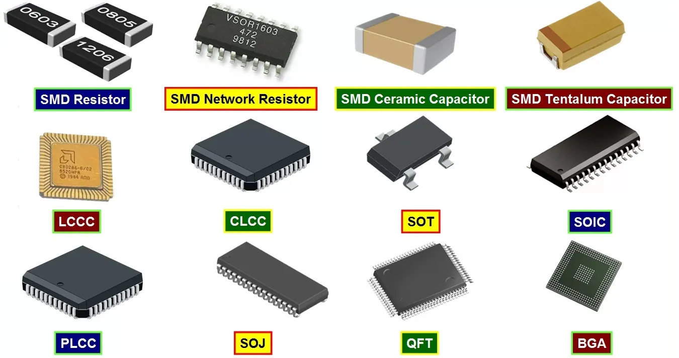
SMD Package Basics
Definition
You often see the term "smd package" when you work with modern electronics. An smd package is a type of electronic component that you mount directly onto the surface of a printed circuit board (PCB). Unlike traditional components with long leads, these packages use short or no leads at all. This design lets you place components closer together, which saves space and supports high-density circuit layouts.
Note: SMD stands for Surface-Mount Device. You will find these packages in almost every compact electronic device today.
Here is a quick comparison of common SMD package types:
| Package Type | Description | Typical Pin Count / Size | Key Features / Applications |
|---|---|---|---|
| SOP | Pins on both sides, L-shape | 8-32 pins | Used for ICs like amplifiers and microprocessors |
| SOIC | Common SMD IC package | Varies | Integrated circuits in many devices |
| SSOP | Smaller than SOIC | Varies | Space-saving for ICs |
| TSSOP | Thin, compact outline | Varies | High pin count in small size |
| SOT | Small transistor package | Few pins | Transistors and small devices |
| QFP | Pins on all four sides | High pin count | Microprocessors, complex ICs |
| QFN | No leads extending out | Varies | Smaller size, better EMI performance |
| PLCC | J-shaped pins around bottom | Varies | Easy chip replacement, less common now |
| BGA | Solder balls on bottom | High pin density | Improved thermal management |
Purpose
You use an smd package to make your electronic designs smaller, faster, and more reliable. These packages help you fit more components onto a single PCB, which is essential for devices like smartphones and wearables. The small size and light weight of SMD components allow you to create high-density circuits and support miniaturization.
-
Short leads or leadless designsreduce resistance and inductance. This means your circuits can run faster and handle higher frequencies with less signal loss.
-
Automated pick-and-place machines assemble SMD packages quickly and accurately. This process lowers labor costs and speeds up production.
-
You save on materials because SMD packages use less metal and plastic. This makes each component cheaper to produce.
-
Surface mounting improves heat dissipation. The package sits directly on the PCB, which helps manage temperature and increases reliability.
-
SMD components have a very low failure rate—less than ten parts per million. This high reliability is important for critical applications.
You can see the main benefits of using SMD packages in electronics:
-
High-density integration and miniaturization
-
Faster and more reliable circuits due to reduced parasitic effects
-
Cost savings from reduced material use and automated assembly
-
Better thermal performance and easier repair
-
Support for high-frequency and high-speed applications
When you choose an smd package, you make your designs more efficient and ready for the demands of modern technology.
SMD Package Features
Size and Weight
You can easily spot the difference in size and weight between SMD packages and traditional components. SMD packages come in a wide range of tiny sizes, which helps you design smaller and lighter electronic devices. For example, the 01005 package measures only 0.4 mm by 0.2 mm. Even larger SMD packages, like the 2920, are still very compact compared to through-hole parts. This small size lets you fit more components on a single PCB and build devices that are lighter and easier to carry.
| SMD Package | Dimensions (mm) | Dimensions (in) |
|---|---|---|
| 01005 | 0.4 x 0.2 | 0.01 x 0.005 |
| 0201 | 0.6 x 0.3 | 0.02 x 0.01 |
| 0402 | 1.0 x 0.5 | 0.04 x 0.02 |
| 0603 | 1.5 x 0.8 | 0.06 x 0.03 |
| 0805 | 2.0 x 1.3 | 0.08 x 0.05 |
| 1206 | 3.0 x 1.5 | 0.12 x 0.06 |
| 2512 | 6.3 x 3.2 | 0.25 x 0.125 |
| 2920 | 7.4 x 5.1 | 0.29 x 0.2 |
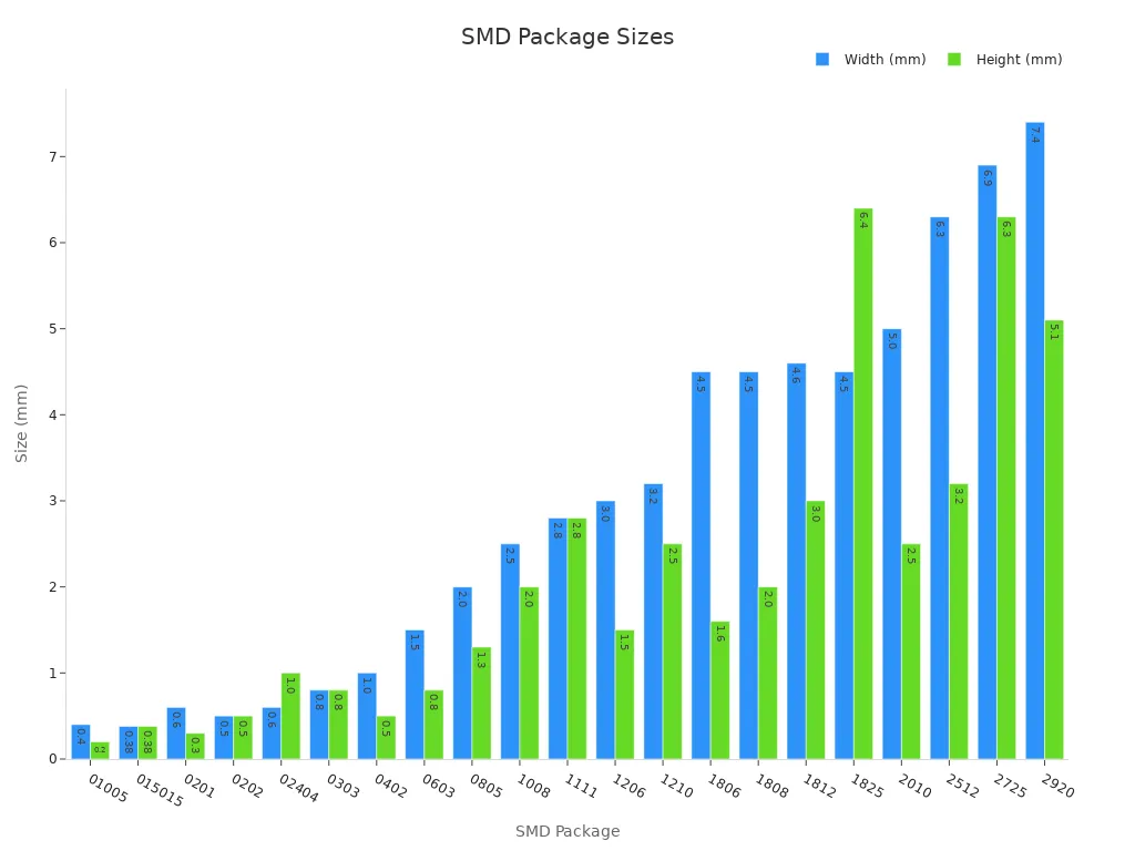
Tip: The small size and light weight of SMD packages make them perfect for smartphones, tablets, and other portable devices.
Lead Structure
You will notice that SMD packages use short leads or sometimes no leads at all. This design helps you reduce unwanted electrical effects, like inductance, which can slow down your circuits. The lead frames inside these packages use special copper alloys mixed with elements such as iron, nickel, or silicon. These materials give the leads strength and keep them stable during assembly.
-
Lead frames in SMD packages provide mechanical support, help move heat away from the chip, and carry electrical signals.
-
Some SMD packages use all-metal lead frames for better heat dissipation and stability. Others use plastics or ceramics for extra strength and protection.
-
High-power SMD packages often use ceramic covers because ceramics handle heat and stress better than plastics.
-
Manufacturers use precise stamping and plating methods to make sure the leads are flat and reliable.
-
Short or leadless designs allow you to place components on both sides of the PCB, making your designs even more compact.
Note: The short leads in an smd package help you build faster and more reliable circuits, especially when you need to fit many parts in a small space.
Reliability
You can trust SMD packages to perform well, even in tough environments. Industry standards like MIL-STD-883, AEC-Q100, and JEDEC set strict rules for testing SMD reliability. These tests check how well the packages handle shock, vibration, and rapid temperature changes.
| Standard | Description | Relevance to SMD Package Reliability |
|---|---|---|
| MIL-STD-883 Method 1015 | Burn-in testing for microcircuits, ensuring robustness under stress. | Includes vibration and thermal cycling. |
| AEC-Q100 | Burn-in testing for automotive electronics. | Ensures components withstand temperature changes, vibration, and electrical noise. |
| IPC-9701A | Guidelines for burn-in process for electronic assemblies. | Provides best practices for stress and reliability. |
| JEDEC Standards | JESD94B (Temperature Cycling), JESD47G (Stress-Test-Driven Qualification). | Used for burn-in and reliability testing in the industry. |
| ISO/IEC Standards | ISO/IEC 60749-25 and IEC 62137-1 for burn-in and reliability assessment. | Ensures global reliability standards compliance. |
SMD packages go through many tests, such as mechanical shock, vibration, and thermal cycling. These tests make sure your devices keep working, even if they get bumped, dropped, or exposed to changing temperatures.
| Test Type | Description | Industry Standard |
|---|---|---|
| Mechanical Shock | Checks if products can handle impacts without damage. | MIL-STD-202 Method 213 |
| Vibration | Tests durability under vibration to find weak spots. | MIL-STD-202 Method 104 |
| Thermal Shock | Exposes parts to quick temperature changes to simulate real-world stress. | JESD22 Method JA-104 |
You benefit from this high reliability in many ways:
-
Your devices last longer and need fewer repairs.
-
SMD packages resist shock, vibration, and electromagnetic interference, so your electronics work well in cars, airplanes, and industrial machines.
-
You can design double-sided PCBs, which means you can fit more features into smaller products.
Callout: SMD packages help you build compact, reliable, and high-performance electronics that stand up to real-world challenges.
SMD vs. Through-Hole
Mounting Differences
You will notice clear differences between SMD and through-hole mounting when you work with PCBs. SMD components sit directly on the surface of the board. You do not need to drill holes for their leads. This makes assembly faster and allows you to use both sides of the PCB for placing parts. Through-hole components, on the other hand, require you to drill holes so their leads can pass through the board. This process takes more time and increases manufacturing costs.
-
SMDs are smaller and lighter, so you can fit more of them on a single board.
-
You can use automated machines to place SMDs quickly and accurately.
-
Through-hole parts need manual or wave soldering, which is slower and less reliable.
-
SMDs usually need soldering on one side only, while through-hole parts require soldering on both sides.
-
Through-hole components provide stronger mechanical bonds, making them better for connectors or heavy parts.
Tip: If you want to build compact and high-speed devices, SMD mounting gives you better results. For parts that face physical stress, like switches or connectors, through-hole mounting works best.
Here is a quick comparison:
| Aspect | SMD (Surface Mount Device) | Through-Hole Mounting |
|---|---|---|
| Placement | On PCB surface, no holes needed | Leads pass through drilled holes |
| Assembly | Automated, fast, cost-effective | Manual or wave soldering, slower |
| Board Density | High, double-sided possible | Lower, single-sided preferred |
| Mechanical Strength | Lower, unless reinforced | High, strong physical connection |
| Repair/Rework | More difficult | Easier, accessible leads |
| High-Frequency Performance | Excellent, low signal loss | Lower, more signal distortion |
Design Flexibility
You gain much more design flexibility with SMD packages. Their small size lets you create ultra-compact layouts and fit more features into your devices. You can use both sides of the PCB, which doubles your available space. Advanced techniques, like via-in-pad and high-density interconnects, help you route signals in tight spaces and keep your circuits clean.
-
SMDs support very small sizes, such as 01005 (0.4mm x 0.2mm), so you can pack more components into less space.
-
Flexible and rigid-flex PCBs let you fold or bend your circuits, which is great for wearables or IoT devices.
-
You can use thermal pads, heat spreaders, and thermal vias to manage heat in dense layouts.
-
Careful trace routing and shielding help you keep signal integrity high, even as you add more parts.
Note: SMD technology allows you to design smaller, lighter, and more complex electronics. You can optimize for speed, reliability, and thermal performance, all while saving space.
When you choose SMD packages, you open up new possibilities for creative and efficient PCB designs. Through-hole parts still have their place, especially for high-power or high-stress applications, but SMDs give you the flexibility to meet the demands of modern electronics.
Types of SMD Package
Common Types
You will find many different SMD package types in electronics. Each type has a special shape and size for a specific job. Some packages work best for tiny resistors and capacitors. Others fit complex chips with many connections. You can see how each package serves a unique purpose in the table below:
| Package Type | Typical Dimensions (mm) | Typical Use Case |
|---|---|---|
| 0201 | 0.6 x 0.3 | Extremely high-density applications |
| 0402 | 1.0 x 0.5 | High-density applications such as mobile devices |
| 0603 | 1.6 x 0.8 | Common size for a wide range of applications |
| 0805 | 2.0 x 1.25 | Easier to handle, general use |
| 1206 | 3.2 x 1.6 | Applications requiring higher power ratings |
| SOD-123 | 2.8 x 1.8 | General-purpose diodes |
| SOD-323 | 1.7 x 1.25 | General-purpose and small signal switching diodes |
| SOD-523 | 1.6 x 0.8 | Small signal diodes for high-density applications |
| SOD-723 | 1.3 x 0.6 | Small signal diodes for very high-density applications |
| SOD-882 | 1.0 x 0.6 | Small signal diodes for ultra high-density applications |
| SOIC | Varies (8-24 pins) | Low-to-moderate complexity ICs |
| SSOP | Smaller than SOIC | Space-constrained applications |
| TSSOP | Thinner than SSOP | Space-critical designs |
| QFP | 32-256 pins | High pin count ICs with pins on all four sides |
| BGA | Hundreds of solder balls | Very high pin count, improved thermal and electrical performance |
| QFN | Contact pads on bottom | Moderate to high pin count, good thermal performance |
| DFN | Contact pads on bottom | Lower pin count, compact size |
You might use a 0201 package when you need to save space in a smartwatch. For a powerful processor, you may choose a BGA package because it handles heat well and connects many pins.
Tip: Picking the right SMD package helps your design work better and last longer.
Size Codes
You will often see SMD packages labeled with size codes. These codes use numbers to show the length and width of the package. For example, a 0603 package measures 1.6 mm by 0.8 mm. The first two digits show the length, and the last two show the width, both in tenths of a millimeter.
-
0402 means 1.0 mm x 0.5 mm
-
0805 means 2.0 mm x 1.25 mm
-
1206 means 3.2 mm x 1.6 mm
Manufacturers use these codes to help you pick the right part for your project. You can quickly match the code to the space you have on your circuit board.
Note: Always check the size code before you order parts. This step makes sure your SMD package fits your design.
SMD and SMT
SMT Overview
You will often see the term SMT, which stands for Surface-Mount Technology. SMT is the process you use to attach electronic components directly onto the surface of a printed circuit board (PCB). You do not need to drill holes for the leads. This method makes your assembly faster, more accurate, and much more efficient.
SMT uses a series of precise steps to build electronic devices:
-
Prepare the PCB with flat copper pads.
-
Print solder paste onto the pads using a stencil.
-
Place SMD components onto the solder paste with high-speed pick-and-place machines.
-
Heat the board in a reflow oven to melt the solder and secure the parts.
-
Inspect the finished board using Automated Optical Inspection (AOI) or X-ray machines.
Tip: Most defects in SMT come from solder paste printing. Careful inspection at this stage helps you avoid problems later.
Here is a quick look at the SMT process and its features:
| Aspect | Description |
|---|---|
| Smallest component size | As tiny as 0201 (0.25 mm x 0.125 mm) |
| Placement speed | Up to 100,000 parts per hour with advanced machines |
| Inspection methods | AOI, X-ray, flying probe, and in-circuit testing for high reliability |
| Cost savings | Automation reduces labor and material costs by up to 50% |
Role of SMD in SMT
SMD packages play a key role in the SMT process. You use SMDs because they are small, light, and easy to place with machines. Their design allows you to fit more parts on both sides of a PCB, which helps you build smaller and more powerful devices.
-
SMDs support miniaturization, letting you create complex circuits in a small space.
-
Automated pick-and-place machines handle SMDs quickly and accurately, reducing human error.
-
SMDs improve performance by reducing lead length, which helps with high-frequency signals and better heat management.
-
You can use SMDs in many industries, such as smartphones, cars, medical devices, and even aerospace.
Note: SMD packages and SMT work together to make electronics more reliable, cost-effective, and ready for the future.
You benefit from this combination through faster production, higher quality, and lower costs. SMT with SMDs also supports environmental goals by reducing material waste and energy use. As technology advances, you will see even more improvements in speed, flexibility, and reliability thanks to this powerful pairing.
You gain many benefits when you use an smd package in your designs. These packages help you build smaller, faster, and more reliable devices. You can see their value in modern electronics through:
-
Automated inspection methods like AOI and X-ray for quality control
-
Burn-in and stress testing to ensure reliability
-
High assembly density and low failure rates
| Aspect | SMD Packages | Traditional Through-Hole Components |
|---|---|---|
| Assembly Density | High (40-60% reduction) | Lower density |
| Failure Rate | Less than 10 ppm | About 50 ppm |
| Production Efficiency | 50% higher | Lower automation |
Understanding these features helps you make better choices in design and manufacturing. You can explore more about advanced packages and their uses in future projects.
FAQ
What does SMD stand for?
SMD stands for Surface-Mount Device. You use these components by placing them directly onto the surface of a printed circuit board (PCB). This method helps you build smaller and more efficient electronic devices.
Why do you choose SMD packages over through-hole components?
You choose SMD packages because they save space, reduce weight, and allow faster assembly. SMDs help you create compact designs and support high-speed circuits. You also benefit from lower costs and higher reliability.
Can you solder SMD components by hand?
Yes, you can solder SMD components by hand using fine-tipped soldering irons and tweezers. You need steady hands and good lighting. For very small parts, you may find it easier to use hot air tools.
How do you identify SMD package sizes?
You identify SMD package sizes by their code, such as 0603 or 0805. The numbers show the length and width in tenths of a millimeter. Always check the datasheet to confirm the exact size.
Are SMD packages reliable for harsh environments?
SMD packages offer high reliability. They resist shock, vibration, and temperature changes. You can use them in cars, airplanes, and industrial machines. Always check the component’s rating for your specific needs.
Written by Jack from AIChipLink.
AIChipLink, one of the fastest-growing global independent electronic components distributors in the world, offers millions of products from thousands of manufacturers, and many of our in-stock parts is available to ship same day.
We mainly source and distribute integrated circuit (IC) products of brands such as Broadcom, Microchip, Texas Instruments, Infineon, NXP, Analog Devices, Qualcomm, Intel, etc., which are widely used in communication & network, telecom, industrial control, new energy and automotive electronics.
Empowered by AI, Linked to the Future. Get started on AIChipLink.com and submit your RFQ online today!


